Home
About us
公司介绍
企业介绍
我们的使命
发展历程
资质专利
合作伙伴
厂区展示
Product
稳压二极管
肖特基二极管
开关二极管
TVS二极管
达林顿三极管
数字三极管
小信号三极管
场效应管(MOS管)
三端稳压器
可控硅
Equipment
生产设备
检测设备
News
公司新闻
行业资讯
Recruitment
招聘英才
Contact us
业务联系
Language
中
EN
CN
Home
About us
公司介绍
企业介绍
我们的使命
发展历程
资质专利
合作伙伴
厂区展示
Product
稳压二极管
肖特基二极管
开关二极管
TVS二极管
达林顿三极管
数字三极管
小信号三极管
场效应管(MOS管)
三端稳压器
可控硅
Equipment
生产设备
检测设备
News
公司新闻
行业资讯
Recruitment
招聘英才
Contact us
业务联系
Market oriented, customer first, sustainable and high quality development
Bluecolour, specialized semiconductor manufacturers.
01
稳压二极管
SOD-123 海鸥脚
400kk/月
01
肖特基二极管
SOD-323 海鸥脚
450kk/月
01
开关二极管
SOT-23
650kk/月
Site display
Factory area
More+
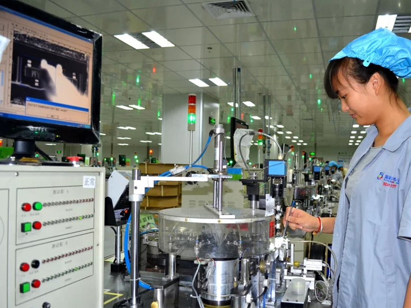
生产设备
生产设备
生产设备
Tel:15351471177
Landline:0825-222 8848-2029
Email:liaoyang@bluecolour.cn
Two-Dimensional code:
About us
Product
Equipment
News
Recruitment
Contact us
四川蓝彩电子科技有限公司
ICP:蜀ICP备2021028478号-1
|
Support:ANGOO